Welcome: Shenzhen leap electronic co.,ltd
Language:
 ∷
∷

∷
∷


In simple terms, PCBA process is a combination of SMT processing and DIP processing. According to the requirements of different production technologies, it can be divided into single-side SMT mounting process, single-side DIP insertion process, single-side mixed process, single-sided paste Assembling and inserting mixing process, double-sided SMT mounting process and double-side mixing process and so on.
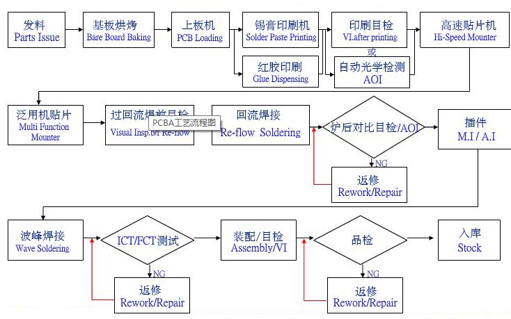
PCBA process flow chart
Single-sided SMT mounting
Single-sided DIP insertion
One-sided mixing
One-side mount and cartridge mixing
Double Sided SMT Mounting
Double-sided mixing
The PCBA process involves the following processes: carrier board, printing, patch, reflow, plug-in, wave soldering, testing and quality inspection.
PCBA process flow chart
Different types of PCBs have different manufacturing processes. The following describes the differences in details for various situations.
1, single-sided SMT mounting
Solder paste is added to the component pad. After solder paste is printed on the bare board of the PCB, the relevant electronic components are mounted by reflow soldering and then reflow soldered.
2, single-sided DIP cartridge
PCB boards that require plug-ins are wave soldered after the production line workers plug in the electronic components. After soldering, the feet can be washed and cleaned. However, wave soldering is less efficient.
3, single-sided mixed loading
Solder paste printing on PCB board, reflow soldering after mounting electronic components, DIP insertion after quality inspection is completed, then wave soldering or manual soldering, if there are few via components, manual soldering is recommended .
4, one-sided mounting and cartridge mixing
Some PCBs are double-sided, one side mounted and the other side mounted. The mounting and inserting process is the same as for single-sided machining, but PCB reflow and wave soldering require the use of fixtures.
5, double-sided SMT placement
Some PCB board design engineers use double-sided mounting to ensure the aesthetics and functionality of the PCB board. One side layout IC components, B surface mount chip components. Make full use of PCB board space to minimize PCB board area.
6, double-sided mixed loading
The following two methods are mixed on both sides. The first method of PCBA assembly is three times heating, and the efficiency is low. It is not recommended to use the red glue process because the pass rate of wave soldering welding is low. The second method is applicable to the case where there are many two-sided SMD components and there are few THT components. Manual welding is recommended. If there are many THT components, wave soldering is recommended.
The above only simplifies the PCBA assembly process of the printed circuit board and displays the manufacturing process in a graphic manner. However, with the gradual optimization of the PCBA assembly process and production process, the failure rate of the PCBA is also continuously reduced, ensuring the production of high-quality finished products. The solder joint quality of all electronic components described above determines the quality of the PCBA board. Therefore, when related electronics manufacturers are seeking PCBA assembly and processing companies, the best requirements are experienced and the level of processing equipment is high.
Contact: Lillian Zhu
Phone: 008613928048496
Tel: 0755-28628518
Email: leappcb@163.com,sales@leappcb.com
Add: Hongtian industry,baoan area,shenzhen city,guangdong ,china
 Lillian
 leappcb